Digital Electronics Workbench
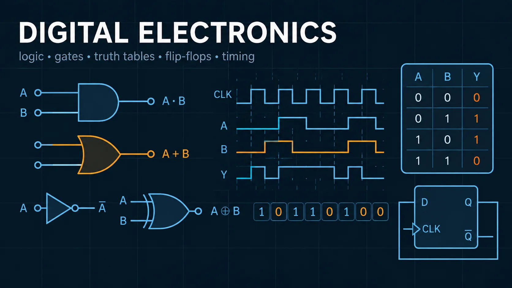
Learn logic gates, Boolean expressions, binary arithmetic, adders, multiplexers, flip-flops, counters, timing, ADCs, DACs, and PWM.
Engineering reference
Digital Electronics: theory, method, and sources
This electrical engineering workspace publishes 5 governing equations, 3 stated assumptions, 1 documented boundary, and 2 sources so the numbers it returns can be checked rather than taken on trust.
How this tool works
Twelve guided modules progress from individual gates and number representation to sequential logic, timing, data conversion, and modulation.
Quantitative plots label time, voltage, frequency, code, and logic-level units explicitly.
Expressions, bit widths, counters, graph samples, restored state, and imported data are bounded before evaluation.
Calculators and topics covered
- digital electronics
- logic
- Boolean algebra
- binary arithmetic
- flip-flops
- ADC
- DAC
- PWM
- truth table
- two’s complement
- ripple carry adder
- multiplexer
- counter
- propagation delay
Core equations
Method and assumptions
Assumptions
- Logic states are ideal binary values unless rise, fall, and propagation times are explicitly entered.
- ADCs and DACs are ideal, monotonic, unipolar converters.
- PWM load-power calculations assume a resistor.
Limitations and design boundaries
- Not a replacement for HDL simulation, metastability analysis, setup/hold timing, clock-domain crossing review, signal-integrity analysis, real converter datasheets, or FPGA/ASIC implementation verification.
Sources and references
Primary sources are preferred for ratings, standards, manufacturer data, and externally defined constants.
- Mano and Ciletti, Digital DesignBoolean logic, combinational circuits, sequential circuits, and counters.
- Floyd, Digital FundamentalsIntroductory digital electronics, data conversion, and timing.